How to make a KiCad footprint

Will get straight to the point and talk at the end of the post.
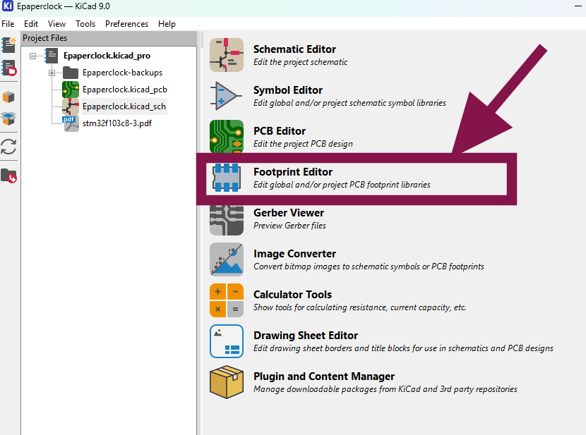
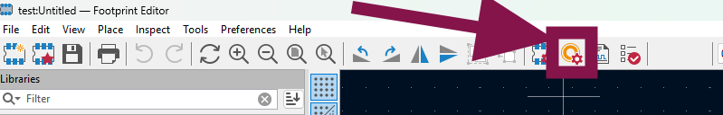
- Enter the footprint editor
- Create a new footprint library, and name it.
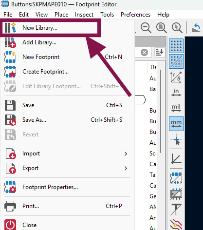
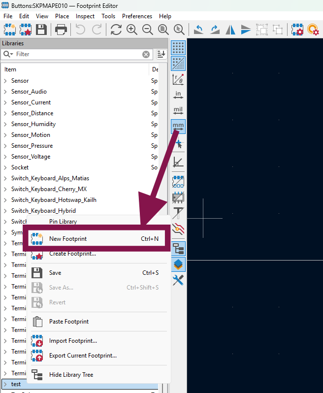
- On the left side select the library you created, right click, and click "New Footprint".
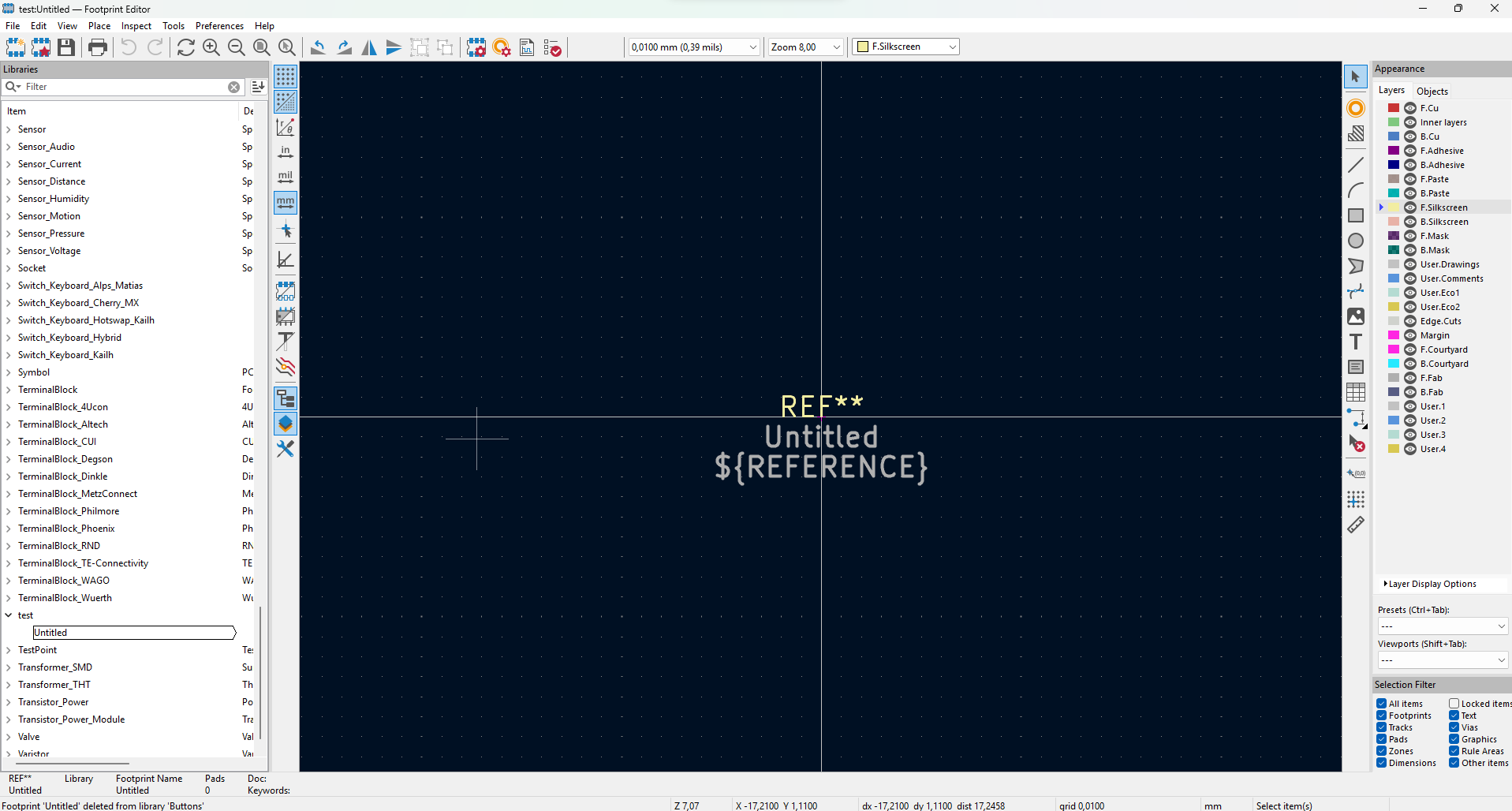
- You will be presented with blank canvas.
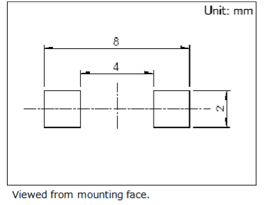
- Acquire datasheet of a desiered component.
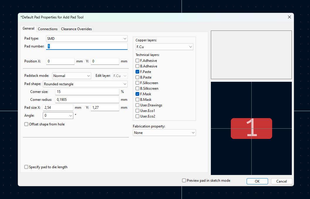
- Edit "Default pad properties".
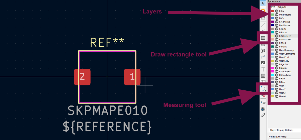
The only important part are pads when you look at it from the PCB perspective. Each pad has a corresponding number, same as symbols have. For example if symbol has connection 1, 2, and 3. You just copy paste 3 pads and edit their dimensions as needed.
- Assemble everything on canvas with tools that are presented to you on the right.

Make sure to sort everything in proper layers.
-F.Courtyard layer is an outline of the component exactly as it is on the PCB (Pink color).
-F.Silkscreen layer is a drawing on the PCB, it's not mandatory (Faint yellow color).
At the end save it.
In one of my projects there was a button that I like to use, and have lots of them, but somehow I couldn't find a footprint for it on the internet. So decision was to make my own footprint. The footprint couldn't be easier, it has just two square pads. Maybe that was the reason there was nothing on the internet, everyone just created their own footprint.